Designing and Building a Two-Stage Audio Amplifier from Scratch
Full technical report on the design, simulation, PCB fabrication and testing of a two-stage audio amplifier using a TL071 active band-pass filter and OPA551 unity-gain output buffer, optimised for an iPhone input and 8 ohm speaker load.
This report describes the design, simulation, testing and implementation of a two-stage audio amplifier optimised for an iPhone 14 Pro Max with a 0.872 Vpp input. A TL071 (Stage 1) performs stereo-to-mono summing, provides 10.67 dB gain and achieves a passband from 6.63 Hz to 28.54 kHz. An OPA551 (Stage 2) drives an 8 ohm speaker at 3 Vpp from a 9 V to 12 V single supply. The amplifier is implemented on a two-layer PCB mounted on an acrylic baseplate.
1. Introduction
This report describes the design, simulation, testing and implementation of a two-stage audio amplifier (see also the project page) capable of accepting an audio input signal from a mobile phone and amplifying it to drive an external speaker. The amplifier was optimised for use with an iPhone 14 Pro Max, with a design input level of 0.872 Vpp at volume step 15 of 16, corresponding to 70% of the maximum measured output at 440 Hz. The target output is 3 Vpp across an 8 ohm speaker load. The system operates from either a 12 V DC power adapter or a 9 V PP3 battery, with an on/off switch and green LED indicator.
A two-stage architecture is employed because no single operational amplifier can simultaneously provide the required voltage gain with active band-pass filtering and the output current necessary to drive a low-impedance speaker load. The first stage uses a TL071 configured as an inverting summing active band-pass filter, combining the stereo left and right input channels into a mono signal, setting the voltage gain to 10.67 dB and defining the passband from 6.63 Hz to 28,540 Hz. The second stage uses an OPA551 configured as a unity-gain voltage follower to provide the current drive capability required to deliver 3 Vpp across the 8 ohm load whilst preserving the voltage established by the first stage.
2. Technical Background
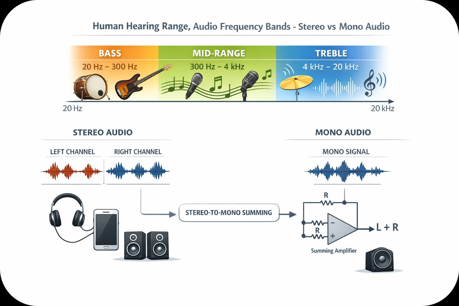
2.1 Human Hearing Range and Stereo vs Mono Audio
The human auditory system can perceive sound across a frequency range of approximately 20 Hz to 20 kHz, although this range varies between individuals and typically narrows with age. Within this audible spectrum, different frequency bands contribute distinct perceptual qualities to sound reproduction. Frequencies in the lower portion of the spectrum, broadly from 20 Hz to approximately 300 Hz, are perceived as bass. The mid-range, spanning approximately 300 Hz to 4 kHz, contains the fundamental frequencies of the human voice and most melodic instruments. The upper portion, from approximately 4 kHz to 20 kHz, is perceived as treble, encompassing the high-frequency content responsible for clarity and brightness of audio.
Human hearing range showing the audible frequency spectrum from 20 Hz to 20 kHz
Consumer audio devices produce stereo audio output consisting of two independent channels, left and right, which carry slightly different audio content. Where a stereo input is to be reproduced through a single mono loudspeaker, the two channels must be combined into a single mono signal. This process is referred to as stereo-to-mono summing and is commonly implemented using an inverting summing amplifier configuration, in which the left and right input signals are each connected to the inverting input of an operational amplifier through separate input resistors of equal value.
2.2 Active Band-Pass Filters
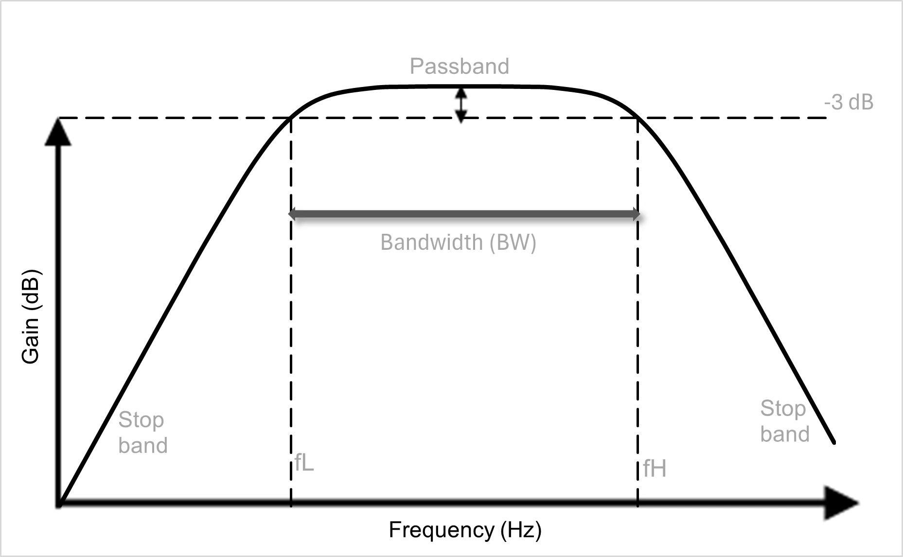
A band-pass filter passes signals between a lower cut-off frequency fL and an upper cut-off frequency fH whilst attenuating all frequencies outside that range. The two cut-off frequencies are defined as the points at which the output signal power falls to half of its maximum value, corresponding to a reduction in voltage gain of 3 dB below the maximum passband gain.
Figure 1: Frequency response of an ideal band-pass filter
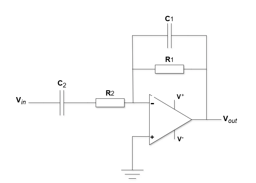
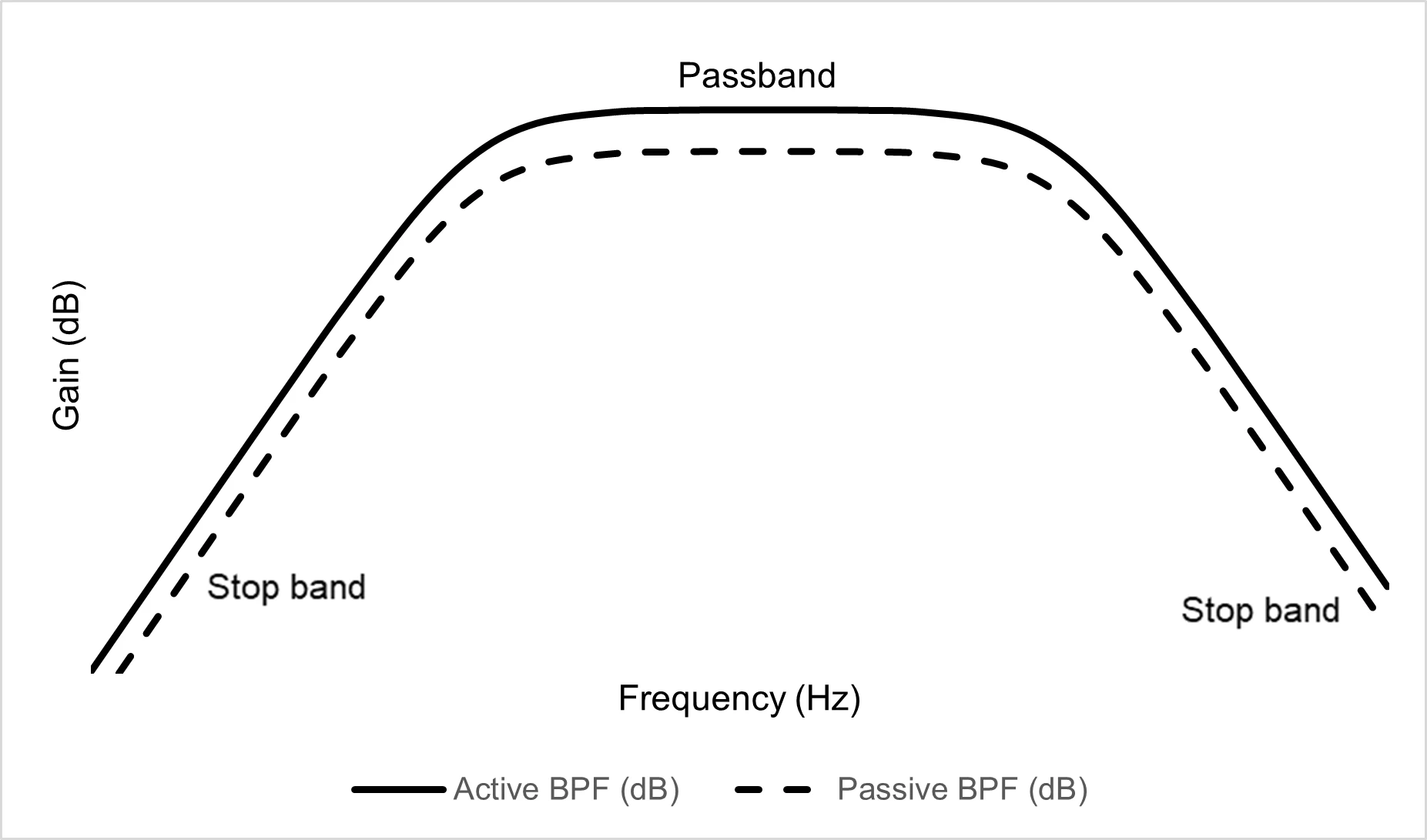
A passive band-pass filter constructed using only resistors and capacitors attenuates the signal within the passband as well as outside it, resulting in a voltage gain of less than unity. An active band-pass filter incorporates an operational amplifier, which provides gain within the passband and allows the overall voltage gain to be set to a value greater than unity. The operational amplifier also provides a low output impedance, isolating the filter from the load and preventing the load from affecting the frequency response.
Figure 2: Active band-pass filter circuitFigure 3: Comparison of passive and active band-pass filter frequency responses
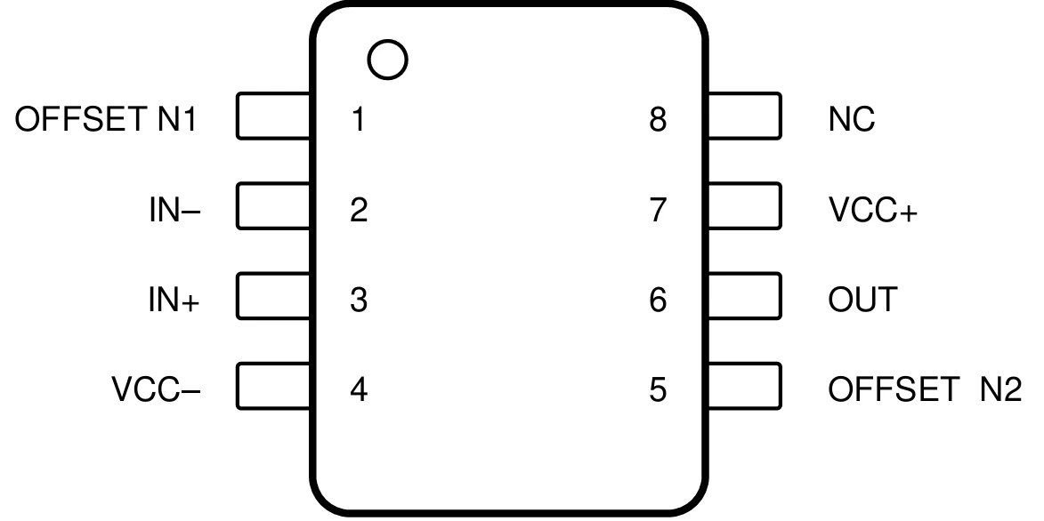
2.3 The TL071 Operational Amplifier
The TL071 is a general-purpose JFET-input operational amplifier. The JFET input stage provides a high input impedance and an extremely low input bias current, minimising the loading effect on preceding signal sources. The device is unity-gain stable and has a gain-bandwidth product of approximately 3 MHz and a slew rate of 13 V/us. The low input noise of 18 nV/sqrt(Hz) and total harmonic distortion of 0.003% are important parameters for high-fidelity audio reproduction. The TL071 operates from a supply voltage range of +/-2.25 V to +/-18 V, making it suitable for both dual-supply and single-supply configurations.
Figure 4: Pin configuration of the TL071 operational amplifier
2.4 The TL071 as an Inverting Summing Active Band-Pass Filter
The TL071 may be configured as an inverting summing amplifier by connecting multiple input signals to the inverting input terminal through separate input resistors of equal value. In this configuration, the output voltage is proportional to the inverted sum of all input signals, weighted by the ratio of the feedback resistance to the respective input resistance. This property is used in the present design to combine the left and right channels of a stereo audio signal into a single mono signal.
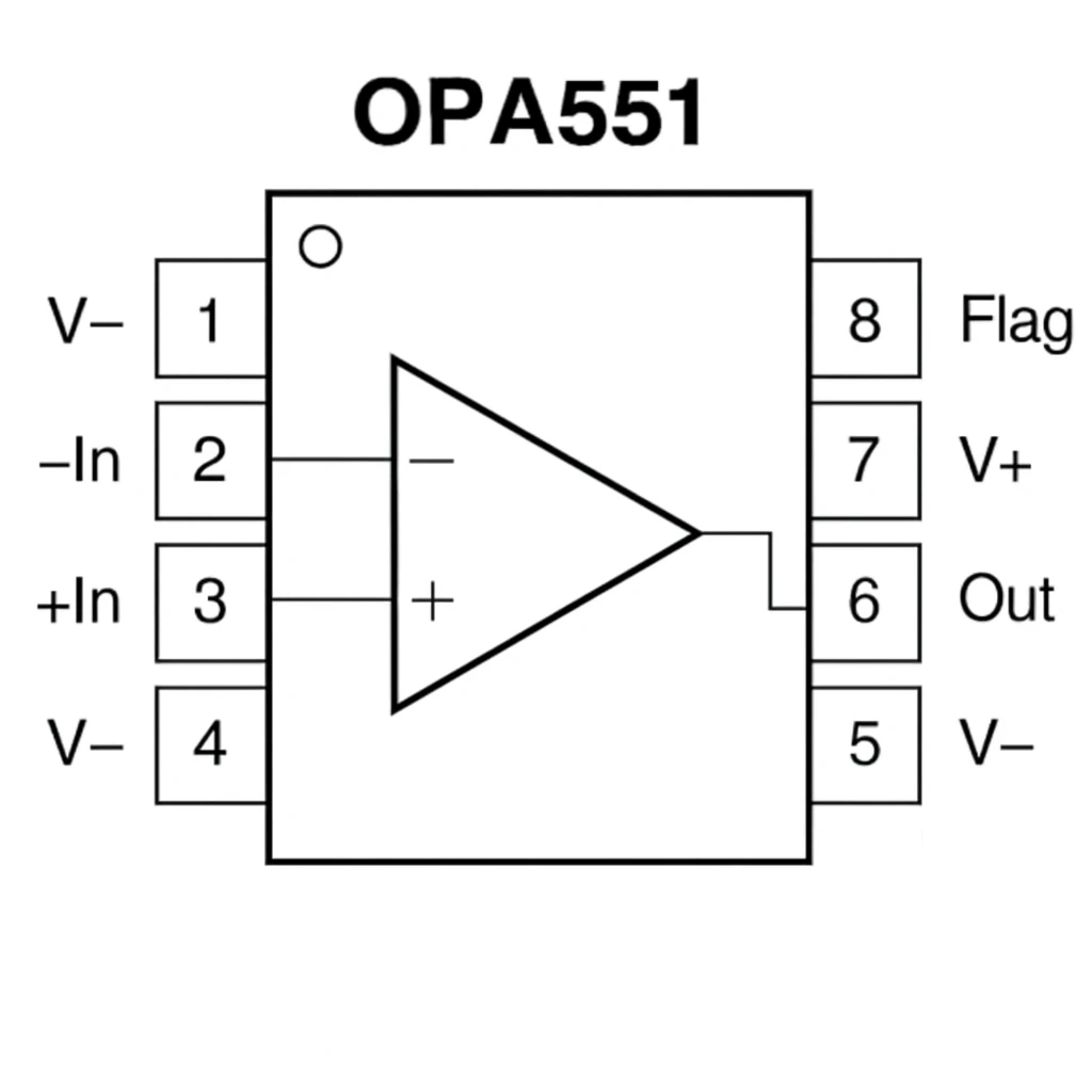
2.5 The OPA551 Operational Amplifier
The OPA551 is a high-voltage, high-current operational amplifier designed for applications requiring large output current capability. It can supply a continuous output current of up to +/-200 mA, making it suitable for directly driving low-impedance loads such as loudspeakers without an additional discrete output stage. The OPA551 has a gain-bandwidth product of 3 MHz and a slew rate of +/-15 V/us. The device is unity-gain stable and operates from a supply voltage range of +/-4 V to +/-30 V.
Figure 5: Pin configuration of the OPA551 operational amplifier
2.6 Two-Stage Amplifier Architecture
The two-stage architecture arises from the differing electrical characteristics of the TL071 and OPA551. The TL071 is well suited to filtering and gain setting due to its low noise and JFET input stage, but its output current capability is limited to approximately +/-10 mA. This is insufficient to drive an 8 ohm loudspeaker at the required output voltage. The OPA551 addresses this limitation with an output current capability of up to +/-200 mA. By combining the TL071 as the signal processing stage with the OPA551 as the current amplification stage, the design exploits the complementary strengths of both devices.
3. Design
3.1 Technical Specifications
Input: 0.872 Vpp (iPhone 14 Pro Max, volume step 15 of 16 at 440 Hz)
Supply voltage: 9 V PP3 battery or 12 V DC adapter
Target output voltage: 3 Vpp across 8 ohm speaker load
Output power: 281 mW
Key ICs: TL071CP (Stage 1 active filter) and OPA551PA (Stage 2 unity-gain buffer)
PCB dimensions: 65 mm x 40 mm, two-layer design in Proteus
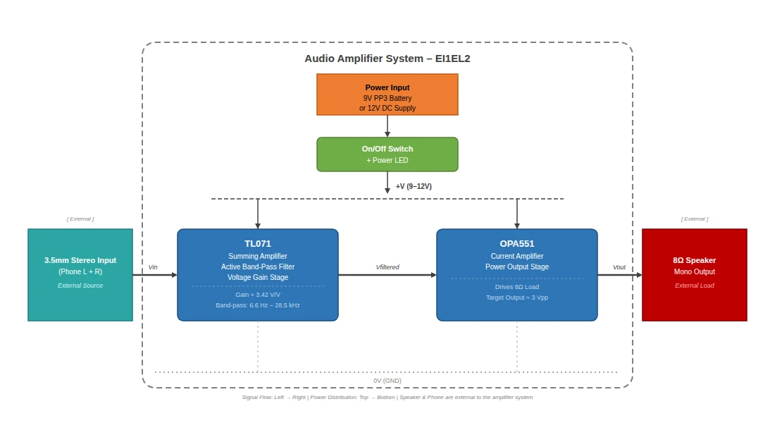
3.2 System Overview
The system accepts a stereo audio input from a 3.5 mm jack socket connected to an iPhone 14 Pro Max and produces a mono amplified output for an 8 ohm speaker. Power is supplied via either a 9 V PP3 battery or a 12 V DC power adapter, passing through an on/off slide switch and a green power indicator LED before being distributed to both amplifier stages.
Figure 6: Top-level block diagram of the two-stage audio amplifier system
3.3 Design Calculations
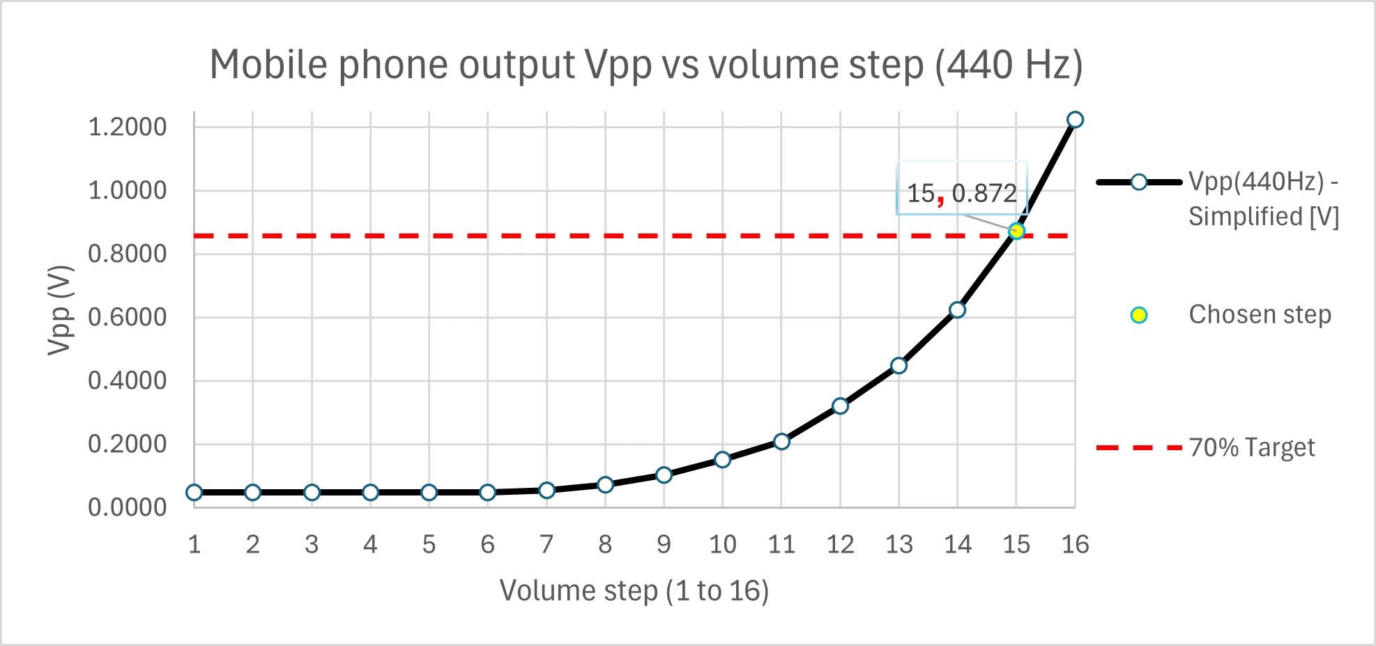
The iPhone 14 Pro Max was characterised by measuring the output voltage at 440 Hz across all 16 volume steps. A frequency of 440 Hz was selected as it corresponds to the international standard musical pitch A4, providing a consistent and reproducible test signal. The design input level was selected at 70% of the maximum measured output of 1.224 Vpp, giving a target of 0.857 Vpp. Volume step 15 of 16 produced an output of 0.872 Vpp, representing an error of 1.77% from the 70% target.
Figure 7: iPhone 14 Pro Max output voltage versus volume step at 440 Hz
The required voltage gain was calculated as Av = Vout / Vin = 3 / 0.872 = 3.44 V/V, equivalent to 20 x log10(3.44) = 10.73 dB. The feedback resistor R1 was given as a fixed value of 82 kOhm. The required input resistor R2 was calculated as R2 = R1 / Av = 82000 / 3.44 = 23.84 kOhm. The nearest preferred stock value of 24 kOhm was selected, giving an actual gain of R1/R2 = 82000/24000 = 3.42 V/V = 10.67 dB.
The lower cut-off frequency fL was given as 5 Hz. The required capacitance C2 = 1 / (2pi x R2 x fL) = 1.326 uF, rounded to 1 uF stock value, giving fL(actual) = 6.63 Hz. The upper cut-off frequency fH was selected as 29 kHz. C1 = 1 / (2pi x R1 x fH) = 66.93 pF, rounded to 68 pF stock value, giving fH(actual) = 28,542 Hz.
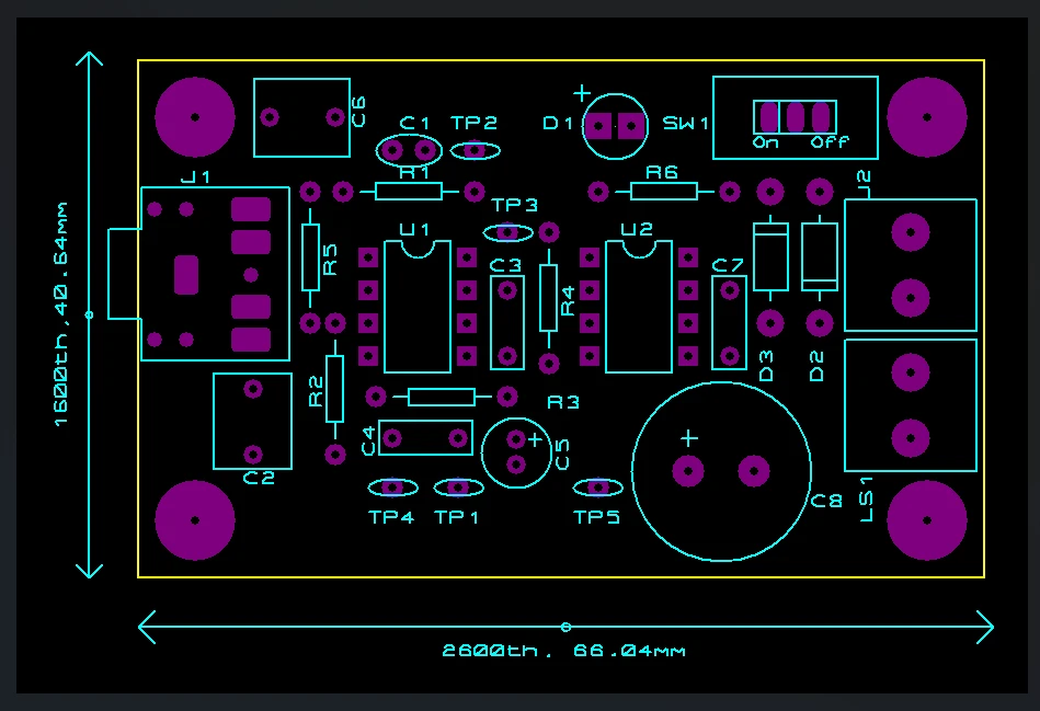
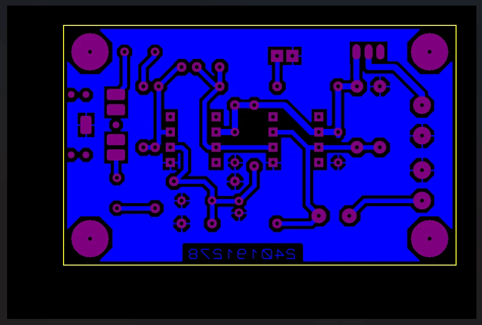
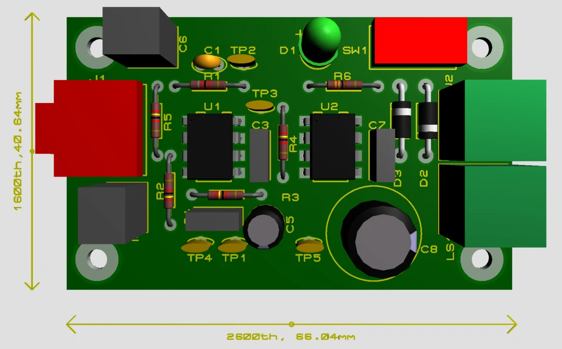
3.4 PCB Design
The printed circuit board was designed in Proteus PCB Layout with overall dimensions of 65 mm x 40 mm. Component placement followed the principle of signal flow from left to right, with the audio input jack socket J1 on the left edge, the power supply terminal block on the top right edge and the speaker output on the bottom right edge. Signal tracks were routed at 0.762 mm and power supply tracks at 1.016 mm. A copper pour was applied to the bottom layer to form a continuous ground plane, reducing ground return impedance and improving electromagnetic compatibility.
Figure 10: PCB top layer showing component placement and silk screenFigure 11: PCB bottom layer showing copper track routing and ground planeFigure 12: Three-dimensional model of the PCB generated in Proteus 3D Visualiser
4. Results
4.1 Breadboard Prototype Testing
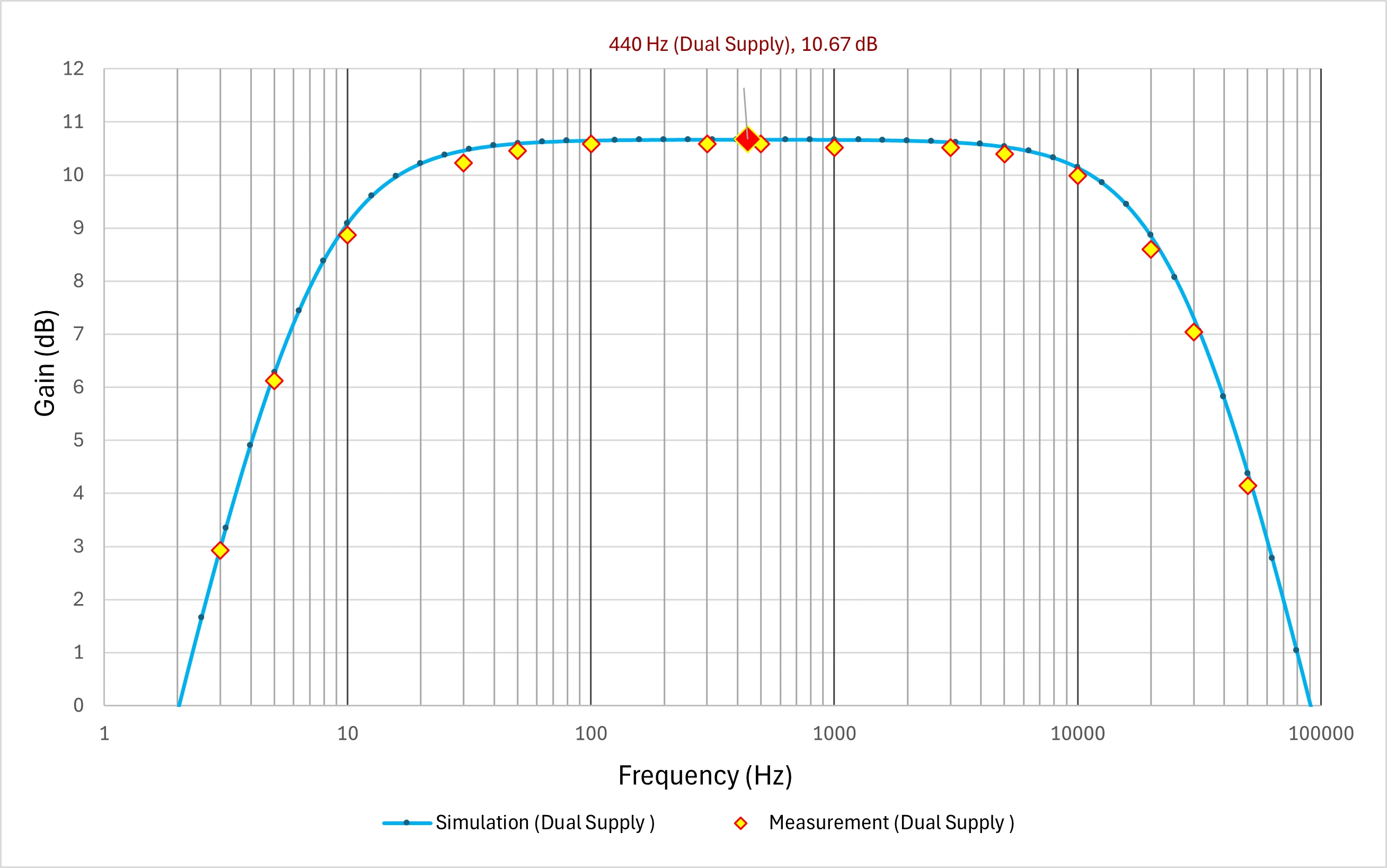
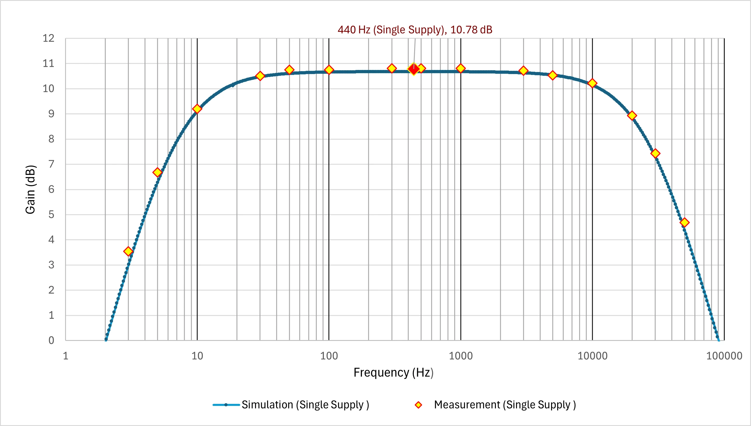
The frequency response of the first amplifier stage was measured on breadboard with a dual +/-9 V power supply. The simulated and measured midband gain at 440 Hz were both 10.67 dB, demonstrating exact agreement. The measured lower cut-off frequency was approximately 7.2 Hz and the upper was approximately 26.0 kHz, both in close agreement with calculated values. Small discrepancies are attributable to component tolerances.
Figure 13: Simulated and measured frequency response of Stage 1 on breadboard with dual +/-9 V supplyFigure 14: Simulated and measured frequency response of the complete amplifier on breadboard with single 9 V supply
4.2 PCB Testing
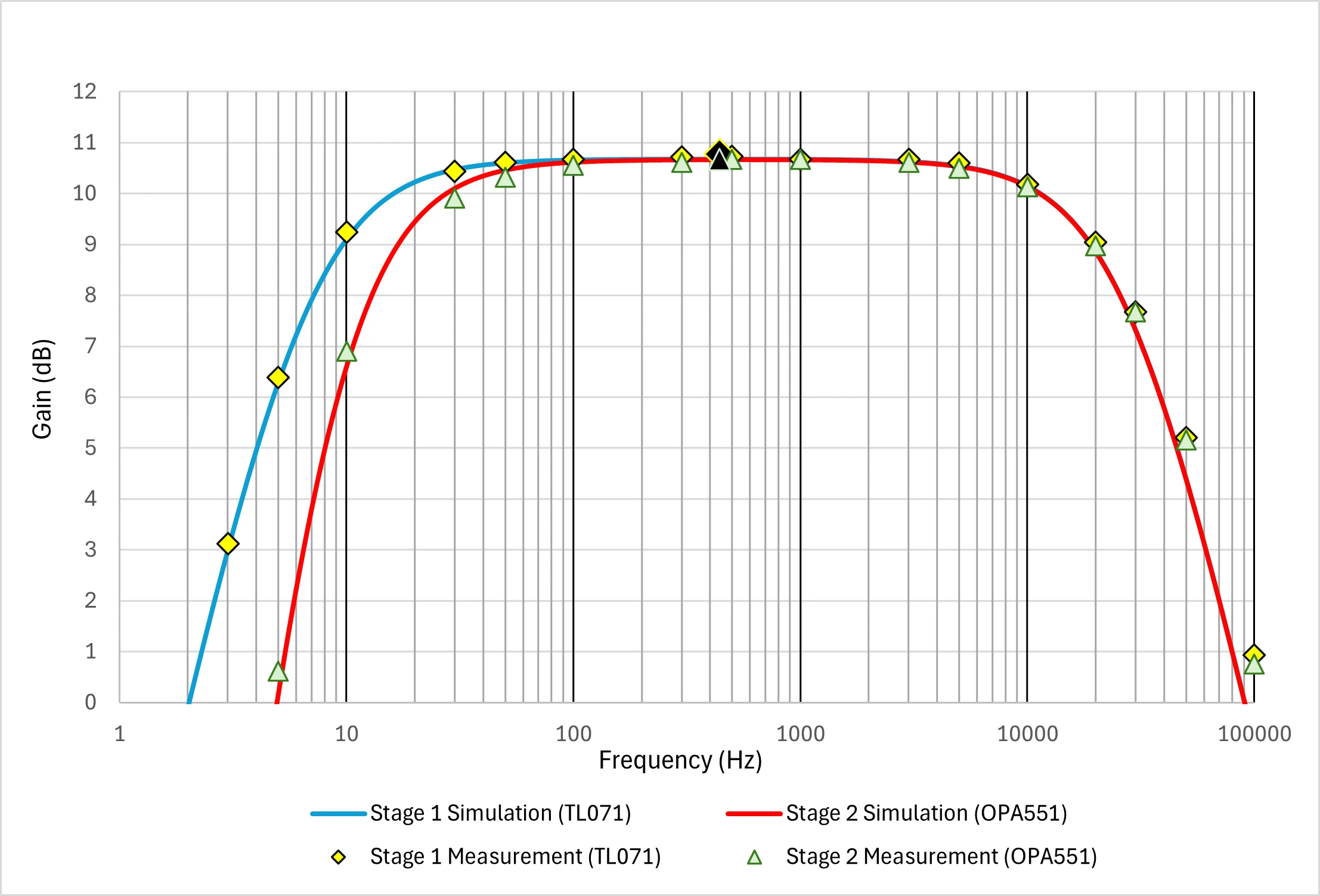
The PCB was tested in stages. Prior to fitting any integrated circuits, a multimeter confirmed that the virtual ground bias voltage of approximately 4.5 V was present at pin 3 of U1. A full frequency sweep from 1 Hz to 100 kHz was performed at each stage. All measured values agreed with calculated and simulated results within acceptable tolerance.
Figure 15: Simulated and measured frequency response of the complete two-stage amplifier on the PCB
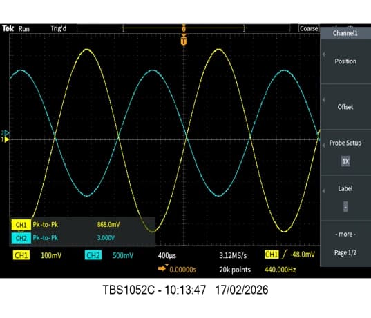
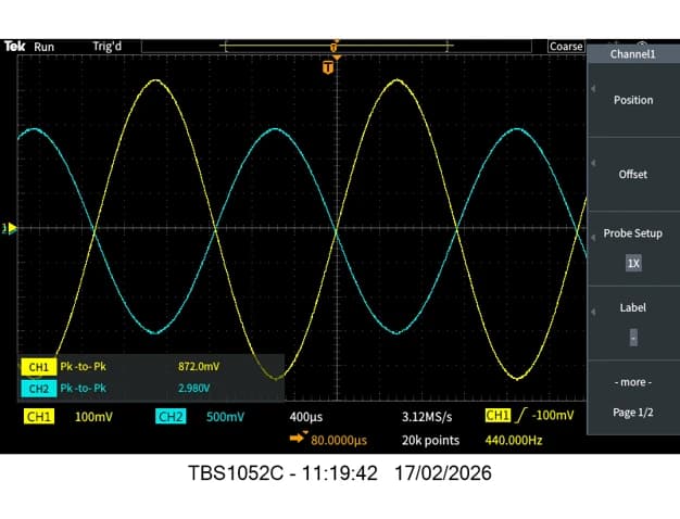
Time-domain testing at 440 Hz: Stage 1 output was 3.000 Vpp for a 868 mVpp input (gain 10.77 dB). Stage 2 output was 2.980 Vpp for a 872 mVpp input (gain 10.67 dB), in exact agreement with the calculated value. All waveforms were clean, undistorted sinusoids confirming linear operation throughout.
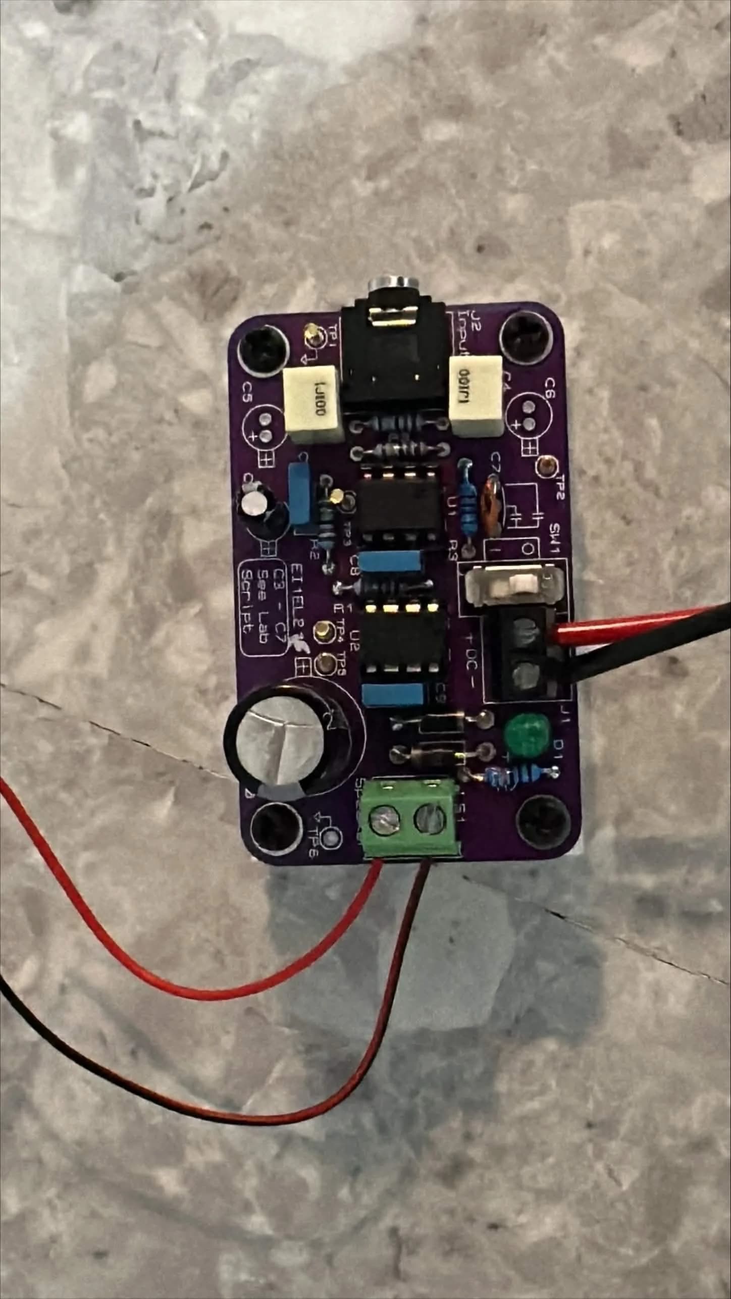
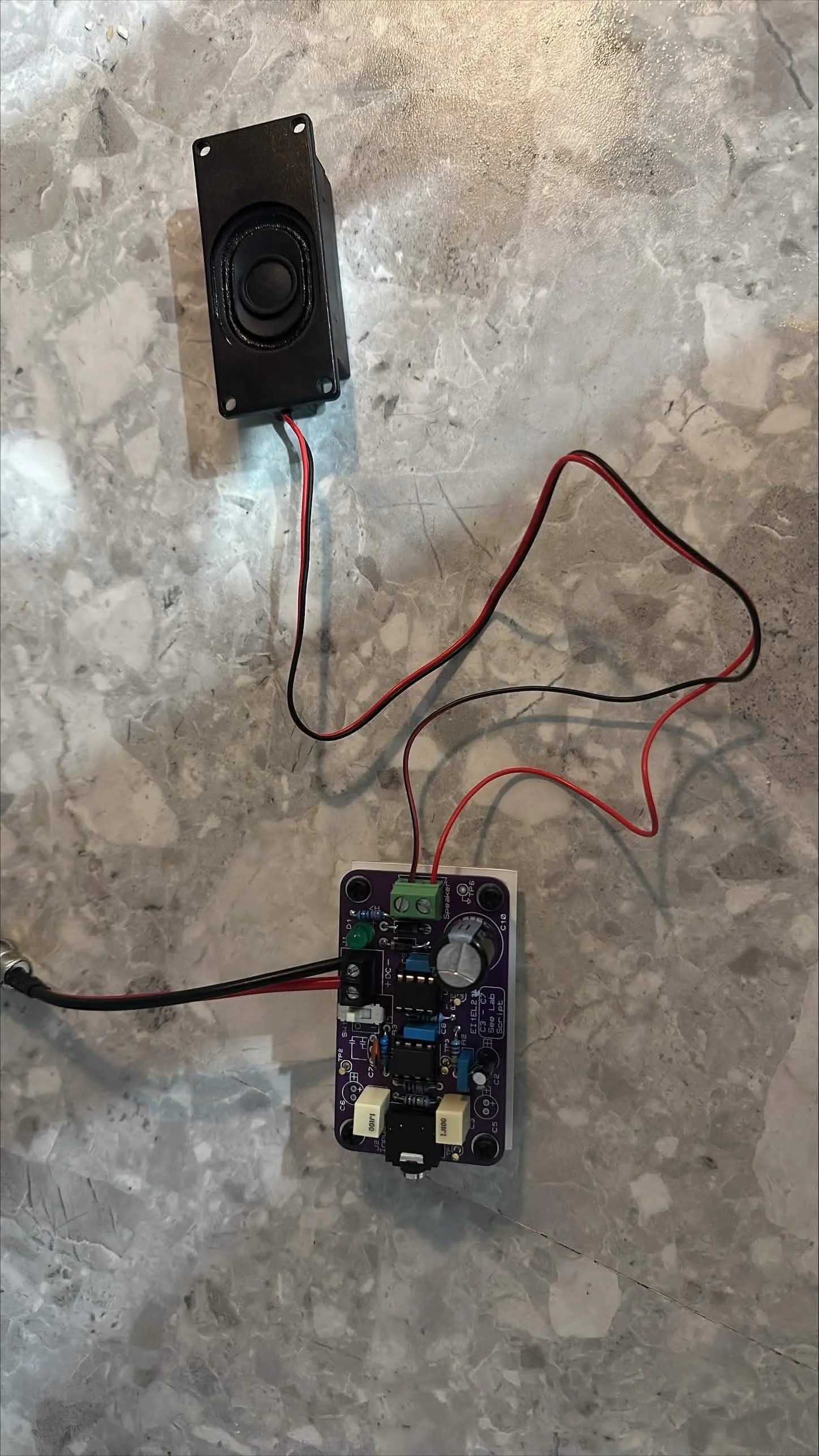
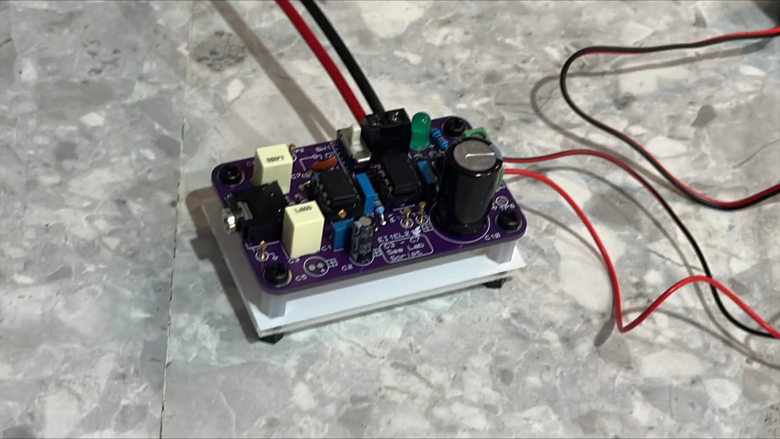
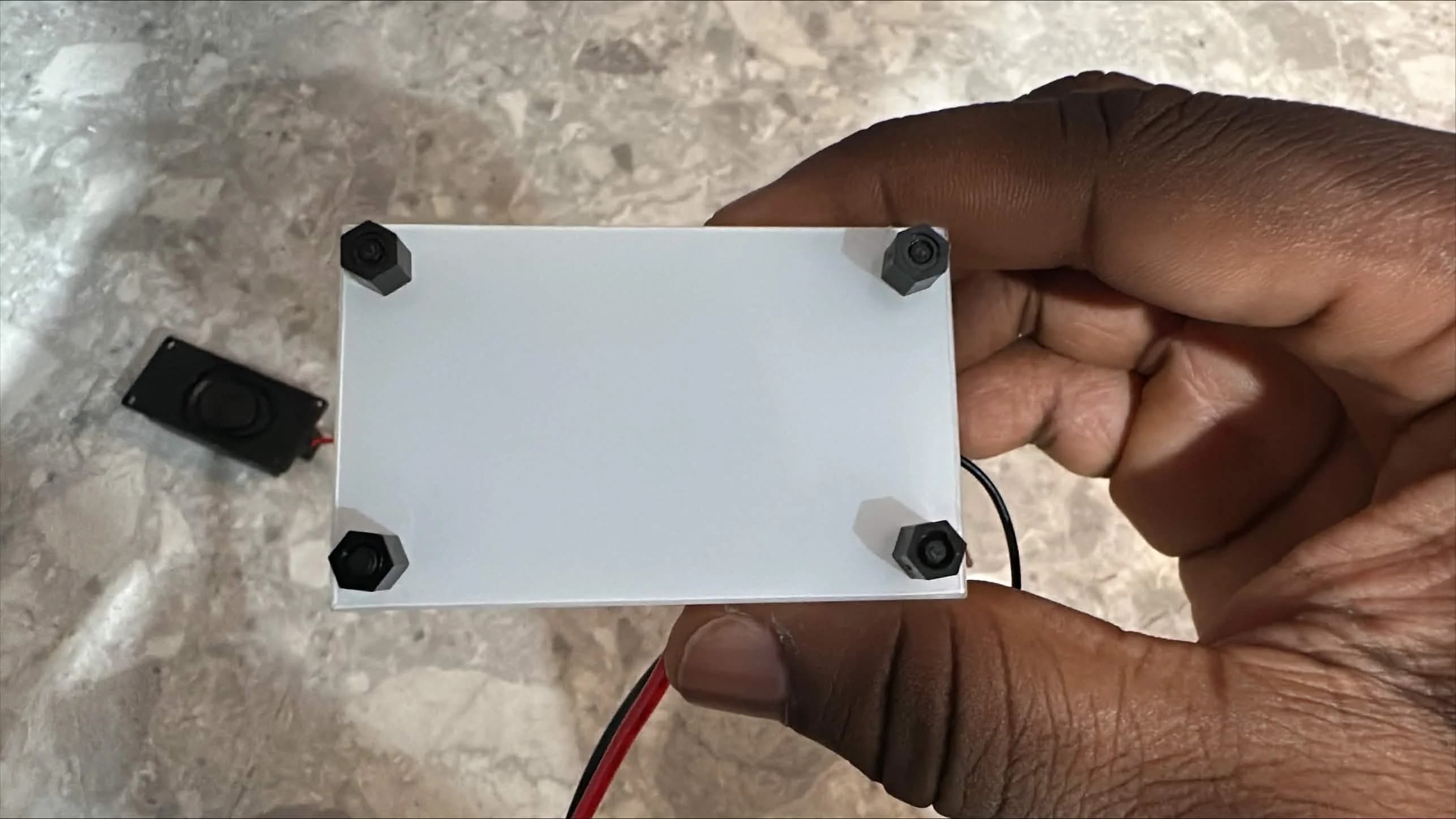
The completed PCB measures 65 mm x 40 mm with a purple solder mask finish, mounted onto a 3 mm acrylic baseplate using four M3 nylon standoffs. U1 and U2 are seated in DIP IC sockets to allow removal and replacement without desoldering. The completed assembly produced an audible 440 Hz tone from the speaker when driven from the iPhone 14 Pro Max at 70% of maximum volume, confirming that the mechanical and electrical assembly is functional.
Figure 17(a): Top view with all components solderedFigure 17(b): Complete system connected to the 8 ohm speakerFigure 17(c): Angled view with LED D1 illuminatedFigure 17(d): Underside showing M3 nylon standoffs and acrylic baseplate
4.4 Evaluation and Conclusions
The design met all key performance targets across simulation and hardware testing. The voltage gain was consistent throughout, measuring approximately 10.67 dB on PCB Stage 2, within 0.14 dB of the calculated value. The 3 Vpp output target was met, with Stage 2 delivering 2.980 Vpp at 440 Hz, agreeing to within 0.67% of the design target.
Possible improvements for future iterations include replacing the screw terminal power input with a dedicated DC barrel jack, designing a dedicated enclosure with a speaker grille, applying conformal coating for moisture resistance and replacing the 3.5 mm jack input with a Bluetooth audio receiver module.
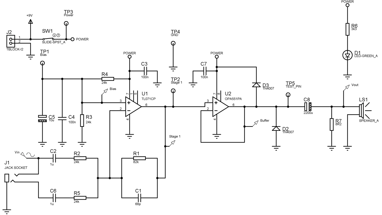
5. Full Circuit Schematic
Figure 18: Full circuit schematic of the two-stage audio amplifier exported from Proteus

Comments
Have a thought, correction or question? Sign in with GitHub - I read every comment and reply where I can.